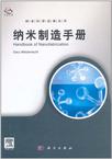
纳米制造手册
出版时间:2011-4 出版社:科学出版社 作者:维德雷希特 编 页数:296
内容概要
现代工业使用的众多器件和系统变得越来越小,有的达到纳米尺寸级别。纳米制造的目标在于构建大量高效低成本的用在组件、器件和系统中的纳米结构。纳米制造是所有纳米技术领域的关键所在,特别是纳米技术在传统的工程和科学领域应用方面。本书覆盖了最重要的纳米制造技术,每章都全面介绍了一种纳米制造技术。适合化工、材料、物理等相关专业的人员阅读。
作者简介
编者:(美国)维德雷希特(Gary Wiederrecht)
书籍目录
编辑顾问委员
前言
编者
1 纳米结构的定向组装 J M MACLEOD,Università degli studi di
Trieste,Trieste,Italy F ROSEI,Université du
Québec,Varennes,QC,Canada
2 有序纳米颗粒超结构的生物调控组装 W L CHENG,S J TAN,M J CAMPOLONGO,M R HARTMAN,J S
KAHN and D LUO,Cornell University,Ithaca,NY,USA
3 表面的手性分子 C J BADDELEY,University of St.Andrews,St.Andrews,UK G
HELD,University of Reading,Reading,UK
4 纳米结构的电子束光刻 D M TENNANT and A R BLEIER,Cornell
University,Ithaca,NY,USA
5 紫外压印光刻在纳米制造中的现状 J CHOI,P SCHUMAKER and F XU,Molecular
Imprints,Inc., Austin,TX,USA S V SREENIVASAN,Molecular
Imprints,Inc.,Austin,TX,USA,University of Texas at
Austin,Austin,TX,USA
6 皮升印刻 E GILI,M CAIRONI and H SIRRINGHAUS,University of
Cambridge,Cambridge,UK
7 分子印刻板:从超分子化学到纳米制造 R SALVIO,J HUSKENS and D N REINHOUDT,University
of Twente,Enschede,The Netherlands
8 分子机械和马达 A CREDI,Università di Bologna,Bologna,Italy
索引
章节摘录
版权页:插图:More specifically, functional inks have enabled awide range of applications in the area of displays andmicroelectronics. For example, light emitting poly-mers (LEPs) have been printed to fabricate polymerlight emitting diodes (PLEDs) [4]. Bottom-gateorganic field effect transistors have also been fabri-cated depositing all the active materials(semiconductor, gate dielectric, and electrodes)using lithography-free printing techniques [5,6].Nevertheless, the development of highly conductive,printable inks necessary to fabricate conductor lineswith low parasitics has proved challenging. Recently,the introduction of inks containing metal nanoparti-cles or metal-containing organic complexes hasallowed to print lines with high conductivity usinglow-temperature processes. In the following, we willdiscuss the different types of metal inks available fordisplay and microelectronic applications. Among the large range of applications of ink-jetprinting of functional materials, in this work we willfocus on display applications (organic light emittingdiodes (OLEDs), liquid crystal displays (LCDs)) andon electronic applications (active matrix backplanes,sensors, radio frequency identification tags (RFIDs),digital lithography and ink-jet etching). It will beclear that for this range of applications the mainfundamental limitation of ink-jet printing is theintrinsic low resolution of the technique. On theother hand, from a manufacturing point of view ithas proven difficult to achieve high yield and deposi-tion uniformity to transfer ink-jet printed electronicdevices to the production floor. In order to improvethe resolution of ink-jet printing, for example, inorder to print short-channel field effect transistors(FETs), a novel approach will be reviewed. This is aself-aligned technique that relies on the movement ofa droplet on a substrate, induced by forces exerted onthe ink by a contrast in surface energy. This can beachieved by pre-patterning high-resolution struc-tures defining areas with different surface energy ona substrate. An alternative, lithography-free approachwill also be discussed.
编辑推荐
《纳米制造手册》为纳米科学进展系列之一。
图书封面
评论、评分、阅读与下载
用户评论 (总计1条)
- 购买时没想到是英文
